Development of High-Power Durable SAW Devices with Epitaxial Aluminum Electrodes
Osamu Nakagawara
[Recipient of the 2010 Richard M. Fulrath Award from the American Ceramic Society]
Surface acoustic wave (SAW) devices are characterized by their capability for compact designs, which has led to their wide installation in mobile devices as frequency filters. Recently, the use of SAW devices in duplexers (antenna branching filters that can perform both transmitting and receiving) , which are an important passive element of communication equipment, has been studied, but a significant technical obstacle has been improvement of the reliability (high-power durability) of the transmission filter where the large power is applied.
In GHz-level high-frequency bands, in particular, microscopic electrode patterning at the 0.5µm level is required for the electrodes, and these designs are susceptible to pattern breakage when power flows. To overcome these practical obstacles in SAW devices, the pattern strength was increased by making the aluminum electrode material into epitaxial film having atomic orientation, and this was successful in enabling a dramatic improvement in the power durability. In lifetime tests that index the power durability, SAW devices that use epitaxial film exhibited a power durability that was a phenomenal 106 times longer than conventional polycrystalline electrodes (equivalent to a durability of 280 years), and these were developed into the world's first W-CDMA SAW duplexer product.
This technology has an extremely high versatility, and currently, it is widely employed for SAW duplexers in Japan and overseas for multiple frequency bands in the third-generation communication standards (UMTS), and it is used throughout the global communications market. This technology provides a significant contribution to the industry by enabling compact and low-profile designs for communication devices, particularly cellular phones.
Also, the discovery of this new crystalline growth pattern has drawn wide recognition as a valuable academic contribution to the field of crystallography, and for this reason, was recognized with the Richard M. Fulrath Award by the American Ceramic Society. Established in 1978 in memory of the great work by the late Professor Richard M. Fulrath, who made tremendous contributions to technological exchanges between Japan and the United States in the ceramic industry fields, the Fulrath award is given to individuals who have made important contributions to the development of ceramic science and technology. In 2010, there were five American and Japanese awardees, and an award symposium and banquet were held at the George Brown Convention Center in Houston, Texas in October 2010. This technology is described in this paper.
Typically, aluminum is used for the electrode film for SAW excitation because of its low resistance and low specific gravity. One drawback of aluminum, however, is that stress migration [1] tends to occur due to the application of repeated stress from SAW propagation, and this results in poor power durability. Because the SAW electrode width is inversely proportional to the operating frequency, the problem of stress migration*1 has become even more noticeable with the greater use of microscopic patterns, which are found in the design of higher frequency devices.
Stress migration is caused by diffusion along the grain boundary primarily consisting of aluminum atoms. In the bulk, the activation energy values for aluminum self-diffusion for single crystals without grain boundaries and for polycrystals with many grain boundaries are 135.1 and 67.55 kJ/mol, respectively, indicating that aluminum atoms in single crystals require larger amounts of energy for diffusion (less susceptible to diffusion) compared to polycrystals. For example, the time required for 100 nm self-diffusion of an aluminum atom at 100°C for single crystals is estimated to be a 109-fold longer than the time for polycrystals with many grain boundaries, which indicates extremely slow atomic movement. This was the reasoning behind our conjecture that the resistance to stress migration could be improved by changing to an epitaxial*2 film where the electrodes have an extremely small amount of grain boundaries within the crystal.
film where the electrodes have an extremely small amount of grain boundaries within the crystal.θrotated Y-cut X-propagation LiNbO3 substrates (called "θrotated Y-X LN substrates" below), which provide superior SAW propagation characteristics, and titanium is used as the intermediate layer which serves as the buffer for reducing the lattice mismatch between aluminum and the substrate. Figure 1 shows a comparison of the pole figure [3] measurement results when using X-ray diffraction (XRD) *3 in the aluminum [200] incidence direction on an aluminum/titanium film and an aluminum single-layer film formed by vacuum evaporation on a LN substrate at θ=64°. Figure 1 (a) shows a ring-shaped diffraction pattern, indicating that [111], which is a close-packed plane in the substrate perpendicular direction, grows for the aluminum single-layer film, and a random polycrystalline film is formed within the [111] plane.
On the other hand, in Fig. 1 (b), clearly-defined six-fold symmetrical spots were found, which indicates that a three-axis oriented epitaxial aluminum film was grown that also had regularity in the [111] plane in addition to the substrate perpendicular direction. In terms of crystallography, aluminum has a face-centered cubic (fcc) structure, and because the [200] pole figure for single-crystal aluminum has a three-fold symmetrical spot, the epitaxial film in Fig. 1 (b) has two single-crystal domains. Because they share the same center of symmetry, this suggests that the growth direction of the aluminum [111] axis is the same, and it has a double domain structure that is rotated 180° within the plane.
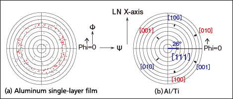
Fig. 1
In addition, particular attention must be paid to the center of symmetry of the six-fold symmetrical spot, that is, the eccentricity of approximately 26° in the aluminum [111] orientation. Because the angle formed by the Z-axis of the θrotated Y-X LN substrate and the line perpendicular to the substrate is 90°-θ, this can be interpreted as a distinctive crystalline growth pattern where the aluminum [111] plane grows with the Z plane of the LN substrate serving as the epitaxial plane. Figure 2 shows a model of the epitaxial aluminum directional relationship on a 64° LN substrate, and this indicates that the aluminum [111] direction and Z-axis of the LN substrate are aligned. Aluminum/titanium films were also formed with different cut angles on the LN substrate, namely, θ=70°and 90° (Z-cut) . As a result, as shown in Fig. 3 (a) and (b) , the angles of eccentricity are 20° and 0°, respectively, and the above-described relationship of aluminum [111] and LN [001] is satisfied.
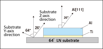
Fig. 2
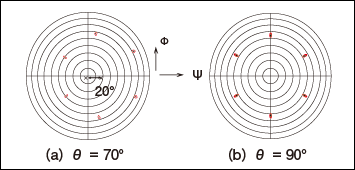
Fig. 3
Figure 4 shows a transmission electron microscope (TEM) image with cross-sections of the aluminum, titanium, and 64° LN planes. This enables confirmation of clear lattice images for LN, titanium, and aluminum. Also, the aluminum/titanium and titanium/LN borders do not show a boundary layer, such as an amorphous layer, indicating that the epitaxial film grows continuously. The incidence (observation) direction of the aluminum film is [-1-12], and the aluminum [111] direction calculated from this nearly matches the direction of the lattice fringe shown in the figure. Also, the pitches in the lattice fringe of the titanium and LN substrate indicate that the planes parallel to the aluminum [111] plane are the titanium [001] plane and LN [001] plane. Furthermore, because the angle formed by the aluminum [111] plane and titanium [001] plane for the film and substrate boundary was 25° to 26°, it was possible to visually confirm the epitaxial growth for the Z plane of LN. The reasons for this type of directional relationship are described below.
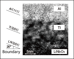
Fig. 4
The consistency of the crystalline lattice for the titanium [001] plane and aluminum [111] plane with respect to the Z plane of LN was considered. The lattice arrangement and interatomic spacing for each plane are shown in Fig. 5. The Z plane of LN, titanium [001] plane having a hexagonal close-packed (hcp) structure, and aluminum [111] plane having a face-centered cubic structure are all close-packed structures*4 and have similar atomic arrangements to those shown in the figure. Furthermore, when the interatomic distances are compared, titanium uses an intermediate value between the LN substrate and aluminum, and so this reduces the mismatch between LN and aluminum. It is thought that the reactivity properties of titanium are added to this lattice consistency for enabling epitaxial growth of metal film on an oxide single-crystalline substrate.
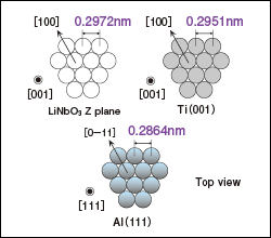
Fig. 5
Next, the epitaxial aluminum film formed on 64° LN is used to manufacture the SAW duplexer, and its power durability was evaluated. Ladder-type filters were used for both the transmitting and receiving sides. Figure 6 shows a schematic diagram of the evaluation system. An acceleration test based on the input power and chip temperature was used for the evaluation. The power-on point was the frequency at the upper-frequency side where the insertion loss becomes 2.5 dB in an atmosphere of 85°C. The power durability evaluation results are shown in Fig. 7. The breakdown times are plotted for values calculated from actually-measured values using the temperature acceleration coefficient. For purposes of comparison, this is also shown together with the power durability for a polycrystalline aluminum electrode, which represents the conventional structure. The triaxial-oriented epitaxial electrode exhibited a breakdown time that was 106 times longer than a conventional electrode (equivalent to a durability of 280 years) , and this value is high enough to enable practical usage. Based on this technology, the world's first SAW duplexer for W-CDMA, which is the third-generation standards, was developed as a product in 2004.
And we successfully developed epitaxial electrodes on LiTaO3 substrates, which are generally used as the LN described in this paper and feature superior temperature characteristics. Currently, this is widely used in SAW duplexers in Japan and overseas for the 2GHz, 1.7GHz, and 800MHz bands for the third-generation communication standards (UMTS) , and more than three million units continue to be produced and sold per month (cumulative total of more than 100million units) .
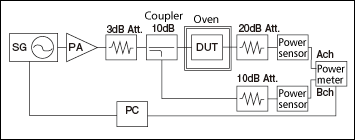
Fig. 6
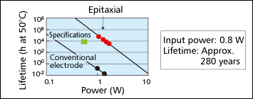
Fig. 7
The epitaxial aluminum obtained here does not show crystal grain boundaries within the field of view in Fig. 4, and the grain boundary is thought to exist in a very small degree at the boundary of grains formed with the double domain formation. The dramatic reduction in the crystal grain boundary due to epitaxial growth is thought to increase the activation energy for the system, resulting in the substantial boost in power durability. The Fulrath Award was presented in recognition of both the high practicability of this technology and the academic value of the discovery of this unique crystalline growth pattern.
Glossary
*1 Stress Migration:
Stress migration is a phenomenon similar to electromigration that occurs in the aluminum thin film of integrated circuits. In stress migration, aluminum atoms move due to internal stress in piezoelectric substrates caused by the propagation of surface acoustic waves, which results in the formation of hillocks, voids, and other defects.
*2 Epitaxial:
Epitaxial refers to growth on a crystal that maintains a fixed orientational relationship on the crystalline substrate which serves as the base. In most thin films, this forms a highly-oriented film where the atoms are extremely aligned.
*3 X-Ray Diffraction (XRD) Pole Figure:
X-Ray Diffraction (XRD) Pole Figure:This is an X-ray diffraction method for obtaining crystal in-plane orientation information. As shown in the figure, the X-ray and detector positions (θ-2θ) are fixed on a certain crystalline plane. The "aluminum [200] incidence direction" mentioned in this paper means that (θ-2θ) are fixed on a certain crystalline plane. The "aluminum [200] incidence direction" mentioned in this paper means that θ and 2θare aligned on the reflective surface of the aluminum [200] . This is rotated to φ=0~360°as needed by changing the tilt ψ of the crystalline plane. The stereographic projection of this series of scans is a pole figure.
*4 Face-Centered Cubic (fcc) Structure, Hexagonal Close-Packed (hcp) Structure:
The close-packed structures where atoms are the most tightly packed is the face-centered cubic (fcc) structure for a cubic crystal lattice and the hexagonal close-packed (hcp) structure for a hexagonal crystal lattice. The [111] plane of the face-centered cubic structure and the [001] plane of the hexagonal close-packed structure are both close-packed planes (shown as aluminum [111] and titanium [001] in the figure).
Original Paper
- "Epitaxially grown aluminum films with titanium intermediate layer on θ rotated Y-X LiNbO3 piezoelectric single crystal substrates." J. Crystal Growth 249 (2003) 497-501.
- "High power durable SAW antenna duplexers for W-CDMA with epitaxially grown aluminum electrodes." 2002 IEEE Ultrasonics Symposium Proc. (2002) 43-46.
- "High Power Durable SAW Filter with Epitaxial Aluminum Electrodes on 38.5°rotated Y-X LiTaO3 by Two-step Process Sequence in Titanium Intermediate Layer." 2003 IEEE Ultrasonics Symposium Proc. (2003) P2L-2.